- 您现在的位置:买卖IC网 > Sheet目录2007 > MAX11040GUU+T (Maxim Integrated Products)IC ADC 24BIT 4CH 38-TSSOP
MAX11040K/MAX11060
24-/16-Bit, 4-Channel, Simultaneous-Sampling,
Cascadable, Sigma-Delta ADCs
29
Maxim Integrated
Referring back to the analog input, since the entire sam-
pling section of the converter also paused for two clock
cycles, the sampling point for sample 5 is also paused
by two clock cycles, possibly creating a small distur-
bance at the SYNC falling edge. This disturbance is fil-
tered with the digital filter, which makes it less distinct.
If the SYNC falling edge occurred during the same XIN
clock period as the DRDYOUT signal, the disturbance
does not affect the periodic timing since the SYNC
falling edge would demand a pause of zero XIN clock
cycles. Hence, connecting the DRDYOUT of the last
converter to the SYNC inputs of many converters, as
illustrated in Figure 13, aligns the sampling of the con-
verters on the first SYNC falling edge, but does not dis-
turb a regular sampling process for future samples.
See the
Multiple Device Synchronization section for dif-
ferent ways to use the SYNC input.
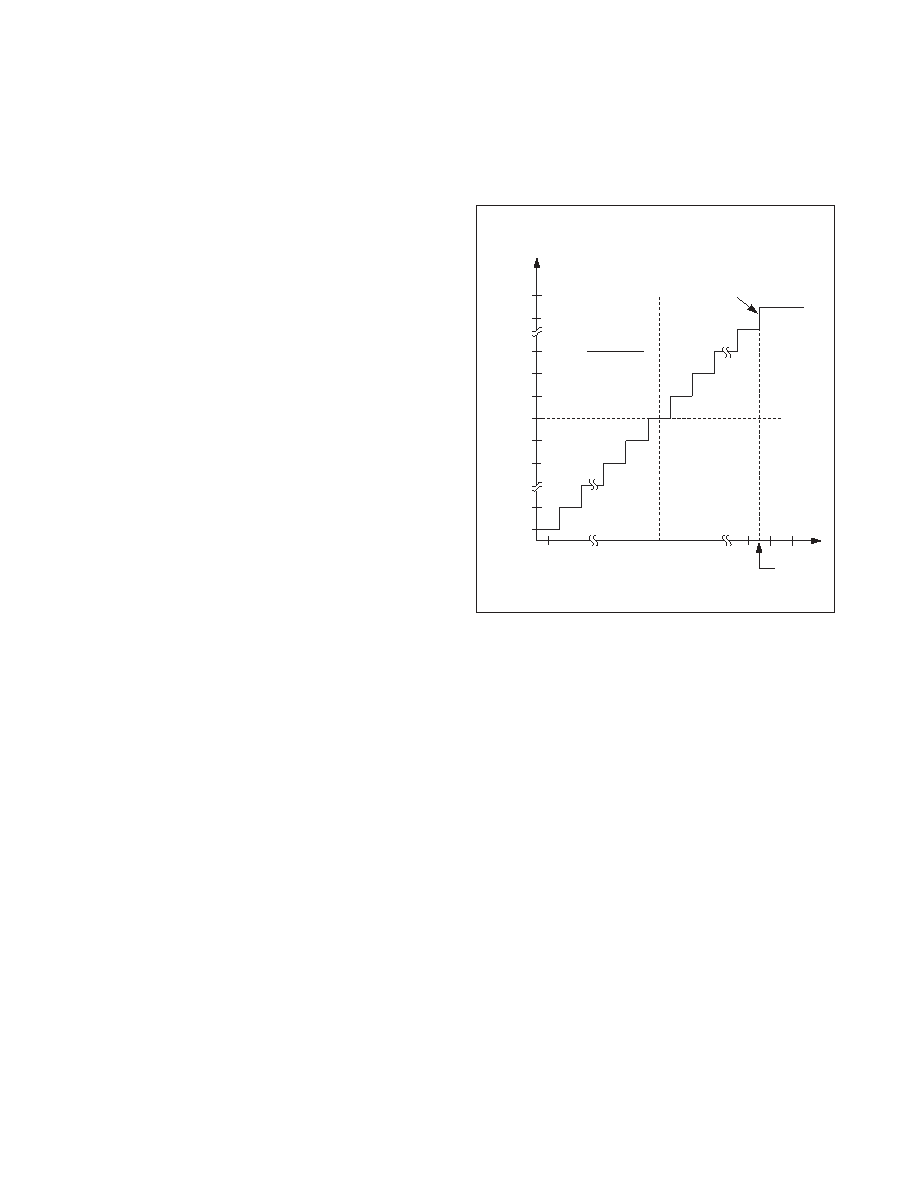
Transfer Function
Figures 17 shows the bipolar I/O transfer function.
Code transitions occur halfway between successive-
integer LSB values. Output coding is binary, with 1 LSB
= (0.88 x VREFIO) x 2/524,288 in 19-bit mode, (0.88 x
VREFIO) x 2/16,777,216 in 24-bit mode, and (0.88 x
VREFIO) x 2/65536 for the MAX11060.
Power-On Reset
The serial interface, logic, digital filter, and modulator
circuits reset to zero at power-up. The power-on reset
circuit releases this reset no more than 1ms after
VDVDD rises above 2V.
OUTPUT CODE
DIFFERENTIAL INPUT VOLTAGE (LSB)
FS
FS - 3/2 LSB
0
-FS
FULL-SCALE
TRANSITION
*N = 19 FOR 19-BIT TRANSFER
FUNCTION,
N = 24 FOR 24-BIT TRANSFER
FUNCTION
FS = +0.88 x VREFIO
ZS = 0
-FS = -0.88 x VREFIO
1 LSB =
2(0.88 x VREFIO)
2N*
100...001
100...000
111...110
000...010
011...111
011..110
000...011
000...001
000...000
111...111
N = 16 FOR MAX11060
Figure 17. ADC Transfer Function
发布紧急采购,3分钟左右您将得到回复。
相关PDF资料
MAX11046ECB+T
IC ADC 16BIT PAR 250KSPS 64TQFP
MAX11046ETN+T
ADC 16BIT SAMPLING 8CH 56-TQFN
MAX11049ECB+
IC ADC 16BIT PAR 250KSPS 64TQFP
MAX1104EUA+
IC CODEC 8BIT 8-UMAX
MAX11100EUB+
IC ADC 16BIT SRL 200KSPS 10UMAX
MAX11101EUB+
IC ADC 14BIT SRL 200KSPS 10UMAX
MAX11102AUB+
IC ADC 12BIT SPI/SRL 10UMAX-EP
MAX1111CPE+
IC ADC 8BIT LP 16-DIP
相关代理商/技术参数
MAX11040K
制造商:MAXIM 制造商全称:Maxim Integrated Products 功能描述:24-/16-Bit, 4-Channel, Simultaneous-Sampling, Cascadable, Sigma-Delta ADCs
MAX11040K_1111
制造商:MAXIM 制造商全称:Maxim Integrated Products 功能描述:24-/16-Bit, 4-Channel, Simultaneous-Sampling, Cascadable, Sigma-Delta ADCs
MAX11040K_12
制造商:MAXIM 制造商全称:Maxim Integrated Products 功能描述:MAX11040K Evaluation Kit/Daughterboard
MAX11040KDBEVKIT
制造商:MAXIM 制造商全称:Maxim Integrated Products 功能描述:MAX11040K Evaluation Kit/Daughterboard
MAX11040KDBEVKIT#
功能描述:数据转换 IC 开发工具 MAX5135/11040/11612 Eval Kit w/ FMC RoHS:否 制造商:Texas Instruments 产品:Demonstration Kits 类型:ADC 工具用于评估:ADS130E08 接口类型:SPI 工作电源电压:- 6 V to + 6 V
MAX11040KEVKIT
制造商:MAXIM 制造商全称:Maxim Integrated Products 功能描述:MAX11040K Evaluation Kit/Daughterboard
MAX11040KEVKIT#
功能描述:数据转换 IC 开发工具 MAX5135/11040/11612 Eval Kit w/ FMC RoHS:否 制造商:Texas Instruments 产品:Demonstration Kits 类型:ADC 工具用于评估:ADS130E08 接口类型:SPI 工作电源电压:- 6 V to + 6 V
MAX11040KGUU
制造商:MAXIM 制造商全称:Maxim Integrated Products 功能描述:24-/16-Bit, 4-Channel, Simultaneous-Sampling, Cascadable, Sigma-Delta ADCs